Author Affiliations
Abstract
Beijing National Research Center for Information Science and Technology (BNRist), Department of Electronic Engineering, Tsinghua University, Beijing 100084, China
A novel thin-film lithium niobate (TFLN) electro-optic modulator is proposed and demonstrated. -silica hybrid waveguide is adopted to maintain low optical loss for an electrode spacing as narrow as 3 µm, resulting in a low half-wave-voltage length product of only 1.7 V·cm. Capacitively loaded traveling-wave electrodes are employed to reduce the microwave loss, while a quartz substrate is used in place of a silicon substrate to achieve velocity matching. The fabricated TFLN modulator with a 5-mm-long modulation region exhibits a half-wave voltage of 3.4 V and a merely less than 2 dB roll-off in an electro-optic response up to 67 GHz.
lithium niobate electro-optic modulator wideband half-wave voltage Chinese Optics Letters
2021, 19(6): 060016
Author Affiliations
Abstract
1 Beijing National Research Center for Information Science and Technology (BNRist), Department of Electronic Engineering, Tsinghua University, Beijing 100084, China
2 Center for Flexible Electronics Technology, Tsinghua University, Beijing 100084, China
3 Flexible Intelligent Optoelectronic Device and Technology Center, Institute of Flexible Electronics Technology of THU, Jiaxing 314006, China
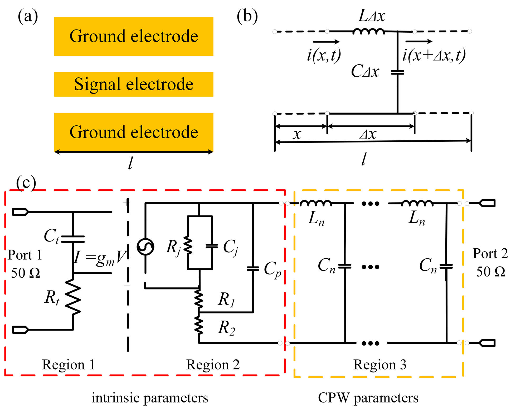
An equivalent circuit model including multi-section distributed parameters is proposed to analyze wideband photodiodes (PDs) with coplanar waveguide (CPW) electrodes. The model helps extract CPW parameters as well as intrinsic bandwidth parameters so that the influence of the CPW structure can be investigated, making it valuable for the design of high-performance PDs. PDs with an inductive 115 Ω impedance CPW are fabricated, and the 3 dB bandwidth is improved from 28 GHz to 37.5 GHz compared with PDs with a conventional 50 Ω impedance CPW.
photodiodes photodetector high-impedance coplanar waveguide Chinese Optics Letters
2020, 18(6): 061301
Tsinghua National Laboratory for Information Science and Technology, Department of Electronic Engineering, Tsinghua University,Beijing 100084, China
Quantum dots in nanowires (DINWs) are considered as important building blocks for novel nanoscale semiconductor optoelectronic devices. In this paper, pure axial heterojunction InGaN/GaN DINWs are grown by using plasma-assisted molecular beam epitaxy (PA-MBE) system. The InGaN quantum dots (QDs) are disk-like observed by scanning electron microscopy (SEM) and transmission electron microscopy (TEM). The diameter of QDs can be controlled by the growth conditions of nanowires (NWs), while the thickness of QDs can be controlled by the growth time of InGaN. Temperature-dependent photoluminescence (TDPL) measurements demonstrate that the PL peak of DINWs with small and uniform sizes shows a general red shift with increasing temperature. However, the PL peak of DINWs with non-uniform sizes shows an abnormal blue shift with increasing temperature, which is due to different internal quantum efficiencies of the DINWs with different sizes.
InGaN quantum dots (QDs) InGaN quantum dots (QDs) nanowires (NWs) nanowires (NWs) photoluminescence (PL) photoluminescence (PL) molecular beam epitaxy(MBE) molecular beam epitaxy(MBE) Frontiers of Optoelectronics
2016, 9(2): 318


